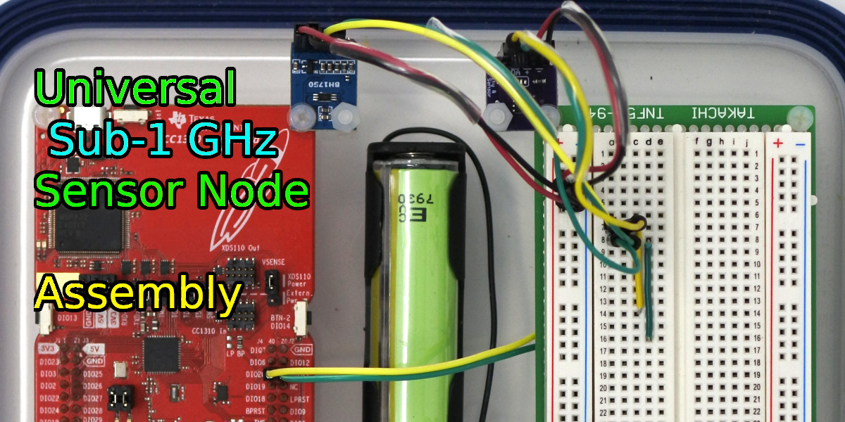
![]()
For the latest news, announcements, comments, views, latest blog post, latest article update and more, visit the Bulletin page.
Series 1: Part 8 - Writing A Skeleton TFT-LCD Display Device Driver
- Details
- Created on Saturday, 28 April 2012 12:19
- Last Updated on Saturday, 28 April 2012 20:04
Abstract
In this part of the series a method of using symbolic logic to represent HDL, when designing the architecture of a hardware algorithm, is introduced. The method is used to develop a modular, skeleton, device driver for TFT-LCD displays in general and the LQ043T3DX02 display (used in the Sony PSP) in particular. The design method introduced is used to generate a display’s horizontal and vertical synchronisation timing signals, by using its (the display's) timing characteristic parameters provided in its datasheet. Finally, by using a color look-up table a method of displaying images on the display is demonstrated.
Read more: Series 1: Part 8 - Writing A Skeleton TFT-LCD Display Device Driver
Altera's DE0 NANO FPGA Development Board: A Review
- Details
- Created on Saturday, 10 March 2012 19:12
- Last Updated on Monday, 30 April 2012 14:59
Introduction
The DE0 Nano development and education board manufactured by Terasic is an entry level, FPGA System-on-Chip (SOC) development board, designed to showcase Altera's Cyclone IV range of FPGAs. Although this board is small in size, at TBD mm x TBD mm, it packs an almighty punch by hosting a EP4CE22F17C6N, Cyclone IV FPGA. That is, an FPGA with 22,320 Logic Elements (LE), although what having 22,320 LEs actually equates to, in terms of ASIC gates, is subject to debate. It can be taken, for now, to mean lots of gates for most beginners and intermediate digital logic designers to experiment with.
Practical examples using the DE0 Nano dev kit, including A DE0 Nano Serial Communication Debug Module, can be found in the tutorials section.
Read more: Altera's DE0 NANO FPGA Development Board: A Review

